| Project | Specification Description |
| Die Attached ethod | Epoxy / Die Attach Film, DAF |
| Bonding Accuracy | X/Y <±20μm, 3σ (epoxy) ; X/Y <±10μm, 3σ (DAF) |
| Cycle Time | 0.45 sec./die (exclude pick up time and bonding time) |
| Wafer Size | 8 ~12 inch |
| Chip Size | 75~ 700 μm / 25~ 75μm (multi-steps unit ) |
| Chip Thickness | 0.75mmx0.75mm ~ 20mmx20mm |
| Substrate /Lead-Frame Size | 100~300mm(L) x 38~100mm(W) x 0.08~1mm(t) |
| Bond Force | 50 ~ 3000g ±10 %;programmable by voice coil motor(V |
| Pattern Recognition System | Black and white, 256 levels of gray scale |
| Wafer Mapping | Standard wafer map format |
| Dispensing method | Epoxy writing /standard pattern application, writing path can be edited |
| Ejector ( die thickness ≥ 75μm) | Single needle ~ Multi-needle |
| Ejector( die thickness < 75um) | Multi-Steps Unit (option) |
| Pre-heating / Bonding area | Room temperature ~ 200℃ Max. |
| Wafer Vision | 3.73x2.8mm~23.83x17.87mm |
| Dispensing Vision | 11.2X8.4mm |
| Bond head Vision | 3.73x2.8mm~23.83x17.87mm |
| Bond Head Rotation Range | ±180゜ |
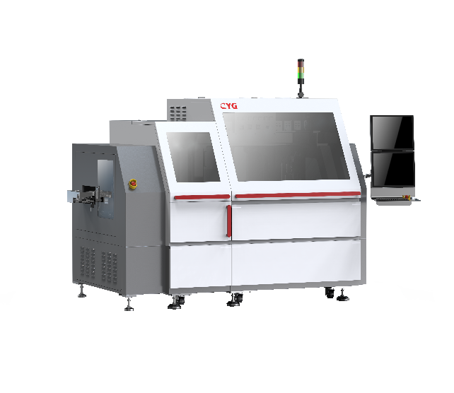
Specification Description
Equipment can be applied to stack-die bonding process. The chip can be directly bonding through epoxy dispensing or by using DAF film through heating and pressure. It can achieve high-level compatibility for bonding of both epoxy and Die Attach Film(DAF).
Contact